1Learning Outcomes
Use truth tables to enumerate the input-output relationships of a basic logic gate and a combinational logic circuit.
Describe the functionality of N-input logic gates (in particular, the 3-input XOR gate).
Practice modular design: compose complex circuits using smaller circuits.
🎥 Lecture Video
🎥 Lecture Video
To design circuits that perform complex operations on binary signals, we must first define primitive operators called logic gates. Logic gates are simple circuits (each with only a handful of transistors) that can be wired together to implement any combinational logic function. In CS 61C we consider logic gates are primitive elements; they are the basic building blocks for our circuits.
The simplest logic gates are binary or unary operators that take as input one/two binary variables and output one binary value.
2Common Logic Gates
Here are some common logic gates. For each we define its name and show (left) its graphical representation and (right) a truth table that defines its function.
AND
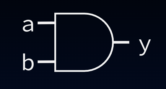
a | b | y |
|---|---|---|
| 0 | 0 | 0 |
| 0 | 1 | 0 |
| 1 | 0 | 0 |
| 1 | 1 | 1 |
OR
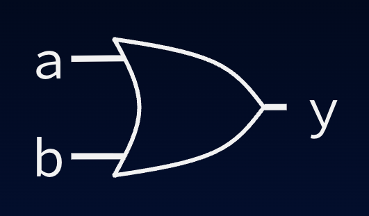
a | b | y |
|---|---|---|
| 0 | 0 | 0 |
| 0 | 1 | 1 |
| 1 | 0 | 1 |
| 1 | 1 | 1 |
NOT

a | y |
|---|---|
| 0 | 1 |
| 1 | 0 |
NAND
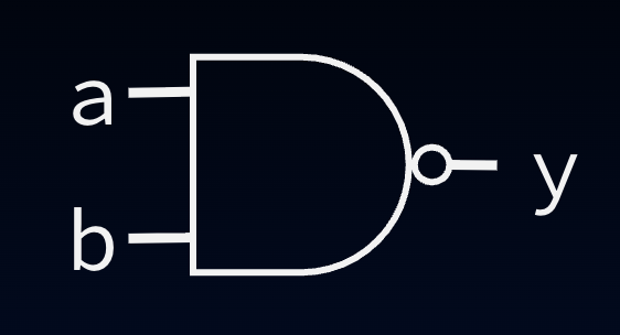
| a | b | y |
|---|---|---|
| 0 | 0 | 1 |
| 0 | 1 | 1 |
| 1 | 0 | 1 |
| 1 | 1 | 0 |
NOR
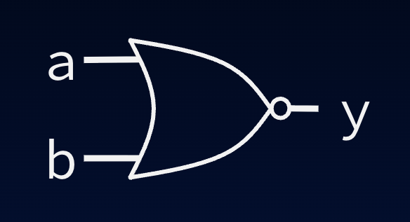
| a | b | y |
|---|---|---|
| 0 | 0 | 1 |
| 0 | 1 | 0 |
| 1 | 0 | 0 |
| 1 | 1 | 0 |
XOR

a | b | y |
|---|---|---|
| 0 | 0 | 0 |
| 0 | 1 | 1 |
| 1 | 0 | 1 |
| 1 | 1 | 0 |
Notes:
AND, OR, NOT and XOR follow from the C bitwise operations you learned eariler.
The NOT gate is commonly called an inverter. Note the “bubble” (circle).
NAND is “NOT” AND. Note the bubble on its output.
NOR is “NOT” OR. Again, note the bubble.
3N-Input Logic Gates
Except for NOT (which is a unary operator), we have shown 2-input versions of these common gates. Versions of these gates with more than two inputs also exist. For performance reasons, the number of inputs to logic gates is usually restricted to around a maximum of four.
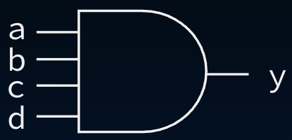
Figure 15:4-input AND gate. The output y is 1 if and only if a, b, and c are all 1.
The function of these gates with more than two inputs is obvious from the function of the two input version, except in the case of the the exclusive-or gate,
Except for NOT (which is unary), we have shown 2-input versions of these gates. Versions of these gates with more than two inputs also exist. However, for performance reasons, the number of inputs to logic gates is usually restricted to around a maximum of four.
The function of these gates is generally self-evident and can deterined by repeatedly composing the equivalent 2-input gate; for example, AND(a, b, c, d) = AND(AND(a, AND(b, AND(c, d)))) = AND(AND(a, b), AND(c, d)), etc. There are a few exceptions; let’s try your reasoning with some quick checks.
What is an N-input NAND?
An N-input NAND is NOT of an (N-input AND).
What is an N-input NOR?
An N-input NOR is NOT of an (N-input OR).
4Combinational Logic Circuit Truth Table
Note that simple logic gates can be wired together to build useful circuits. In fact, any combinational logic block can be implemented with nothing but AND, OR, and NOT logic gates.
However, to understand what a circuit actually does, we need more than just its circuit diagram: we need a concise description of its operation. Let’s first try with truth tables.
To generate a truth-table from a given circuit, we need to evaluate it for input combinations.
So...what does this circuit do? Importantly, we note that the outputs of the two AND gates will never both be 1, so we could have replaced the OR gate with an XOR gate.
After some thought, we may realize that this combinational logic circuit may actually be succinctly described as a compare: Take two inputs and returns 1 if the two inputs are equal and 0 otherwise.
If we wanted to use this compare circuit in other circuits, we can! Just represent it as a combinational logic block, as below:
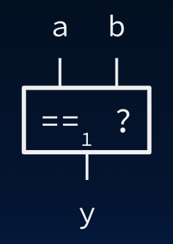
Figure 17:Bitwise compare circuit; a block representation of the mystery circuit in Figure 16.
5Composing Circuits: 32-Bit Comparator
We would like to a circuit that compares two 32-bit values; this 32-bit compare circuit can be used in our processor to implement the equality comparison for the RV32I instruction beq rs1 rs2 Label.
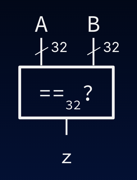
Figure 18:32-bit compare circuit.
Compare this new 32-bit compare circuit(Figure 18) with our previous 1-bit compare circuit (Figure 17):
The value
Ais a 32-bit value, because of the wire bundle (the wire is marked with a notch). Similarly, valueBis 32-bits.The value
zis a 1-bit value.
Functionally, z is 1 only if all of A’s bits are equal to all of B’s bits. In other words, we can perform 32 bitwise comparisons, then AND them together. The underlying circuit for our compare block is therefore as follows:
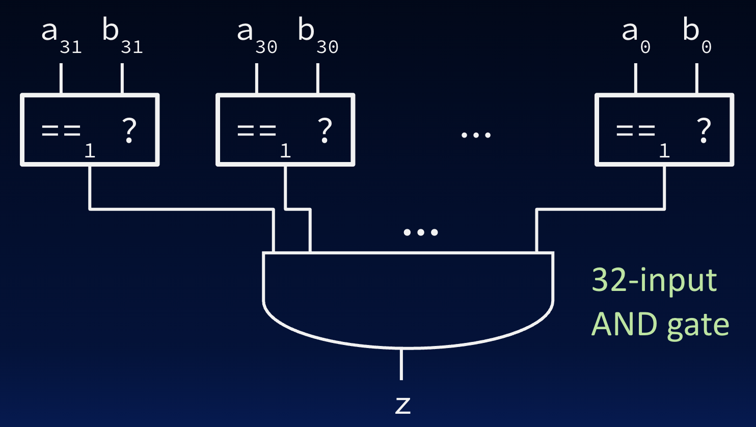
Figure 19:32-bit compare circuit diagram, assuming we have implemented the bitwise compare circuit. The 32-input AND gate can be implemented recursively with 2- or 4-input AND gates.